Professional and high-quality metal alloys, ceramic products and concrete additives | RBOSCHCO

Silicon carbide (SiC), as the third-generation wide bandgap semiconductor material, plays a core role in semiconductor, new energy, industrial manufacturing and other fields due to its excellent characteristics such as high temperature resistance, high pressure resistance, high frequency, and low loss. The derived silicon carbide wafers, silicon carbide ceramics, and silicon carbide heating elements are important application forms of silicon carbide materials, with accelerating technological iterations and expanding practical scenarios.
Fundamentals and core advantages of silicon carbide materials
Silicon carbide is a covalent crystal composed of silicon and carbon elements, with a unique crystal structure. Its core advantages determine the application value of its derivative products and are also the core support for technological development. Compared with traditional silicon materials, the bandgap width of silicon carbide is more than three times that of silicon, the breakdown electric field strength is ten times that of silicon, and the thermal conductivity is three times that of silicon. At the same time, it has excellent chemical stability and mechanical strength, and is not easily corroded or deformed.
Based on these advantages, silicon carbide wafers have become the core substrate for high-end semiconductor devices. Silicon carbide ceramics are suitable for extreme industrial scenarios due to their high temperature resistance and wear resistance. Silicon carbide heating elements rely on efficient thermal conductivity and high temperature resistance to achieve energy-saving heating. The three complement each other and cover multiple core areas from high-end electronics to industrial manufacturing, promoting the upgrading of related industries towards high efficiency, energy conservation, and high-end direction.

Technological development and practical application of silicon carbide wafers
1.Technological Development History and Core Breakthroughs
As the core carrier of silicon carbide semiconductor, the technological development of silicon carbide wafers revolves around “large size, high purity, and low defects”. Early silicon carbide wafers were mainly 2-inch and 4-inch, which had problems such as small size, high defect rate, and high cost, limiting their large-scale application. With technological iteration, large-scale production of 6-inch wafers has been achieved, 8-inch wafers are gradually maturing, and 12-inch wafers have become a research and development hotspot. The expansion of size has greatly improved the integration of semiconductor devices and reduced unit device costs.
The core technological breakthroughs focus on crystal growth and wafer processing, optimizing vapor deposition processes to reduce dislocation and defect density in wafers, improve wafer flatness and purity, and meet the preparation needs of high-end semiconductor devices. At the same time, the upgrade of doping technology has achieved precise preparation of N-type and P-type silicon carbide wafers, adapting to the application scenarios of different types of semiconductor devices.
2. Practical application scenarios
The practical application of silicon carbide wafers mainly focuses on the semiconductor field and is the core substrate of power semiconductor devices and RF devices. In the field of new energy vehicles, it is widely used to prepare on-board power modules, improve the range and charging efficiency of vehicles, and reduce energy consumption. Currently, it has been widely used in inverters and controllers of new energy vehicles; In the field of new energy generation, it is used for photovoltaic inverters and wind power converters to improve energy conversion efficiency and adapt to high-voltage and high-frequency working scenarios; In the field of 5G communication, it is used for RF devices to meet the high-frequency and low loss requirements of 5G communication, improve the stability and transmission speed of communication signals. In addition, it is also applied in aerospace, high-end equipment and other fields to prepare high-temperature resistant and radiation resistant semiconductor devices.
Technological Development and Practical Application of Silicon Carbide Ceramics
1.Technological Development History and Core Breakthroughs
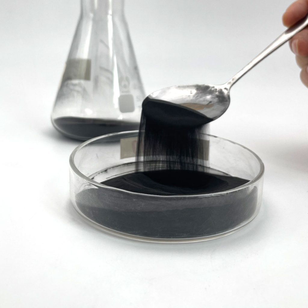
Silicon carbide ceramics are a new type of ceramic material made from silicon carbide as the main raw material and sintered at high temperatures. The core of its technological development is to improve sintering density, toughness, and processing performance. Early silicon carbide ceramics had problems such as difficult sintering, strong brittleness, and easy cracking, which limited their application scope. With the upgrading of sintering technology, processes such as atmospheric pressure sintering, hot pressing sintering, and reaction sintering are continuously optimized, effectively improving the density and toughness of silicon carbide ceramics, reducing sintering temperature, and lowering production costs.
Core technological breakthroughs include composite modification technology, which further enhances the mechanical strength and thermal shock resistance of silicon carbide ceramics by adding auxiliary materials such as carbon fiber and silicon nitride. The upgrade of precision machining technology has achieved high-precision molding and processing of silicon carbide ceramics, enabling the preparation of complex-shaped ceramic components to meet the application needs of different scenarios.
2.Practical Application Scenarios
Silicon carbide ceramics, with their high temperature resistance, wear resistance, and corrosion resistance, are widely used in extreme industrial scenarios and high-end equipment fields. In the field of metallurgy, it is used to prepare high-temperature furnace linings, crucibles, nozzles and other components, resist the corrosion and wear of high-temperature molten metals, and extend the service life of equipment; In the field of mechanical processing, it is used to prepare cutting tools and grinding tools, which have high hardness and strong wear resistance, and can perform precision machining on hard materials, improving machining efficiency and accuracy; In the aerospace field, it is used to prepare high-temperature protective components and engine parts for spacecraft, to resist extreme high and low temperature environments in space and airflow erosion; In the field of environmental protection, it is used to prepare filter materials that can efficiently filter high-temperature, corrosive exhaust gases and wastewater, improving the effectiveness of environmental governance.
Technological development and practical application of silicon carbide heating elements
1.Technological Development History and Core Breakthroughs
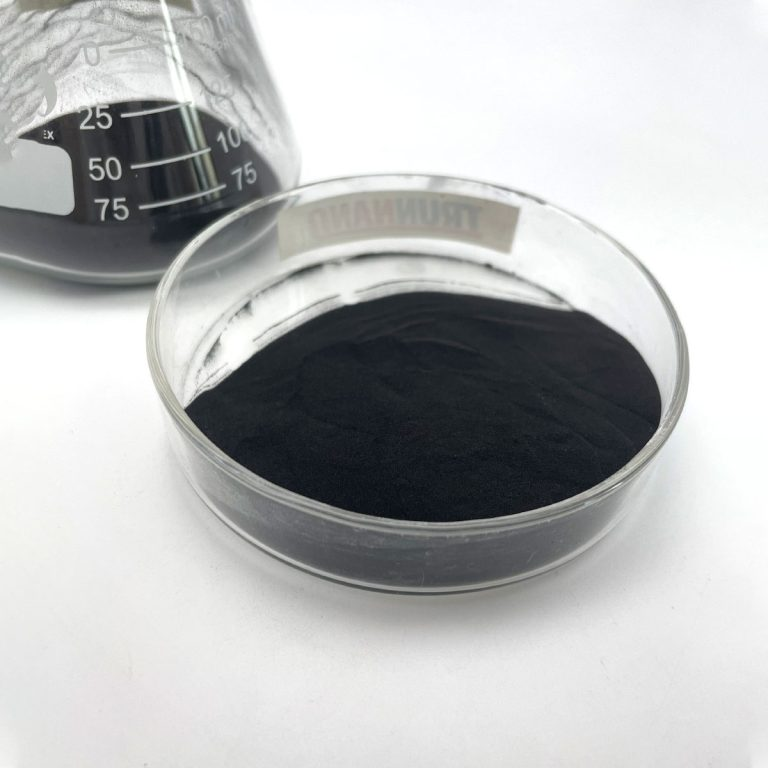
Silicon carbide heating element is a new type of high-temperature heating device made from silicon carbide as the core material, which is formed and sintered. Its technological development core is to improve heating efficiency, service life, and temperature stability. Early silicon carbide heating elements had problems such as uneven heating, short service life, and limited high temperature resistance, and were mainly used in medium and low temperature scenarios. With the upgrading of material preparation and sintering technology, the highest operating temperature of silicon carbide heating elements can reach over 1600 ℃, significantly improving heating uniformity and extending their service life to thousands of hours.
Core technological breakthroughs include improving raw material purity, reducing impurity content, and minimizing energy loss during the heating process; Optimization of the molding process, using techniques such as isostatic pressing to ensure a uniform structure of heating elements and improve heating stability; Surface modification technology enhances the anti-oxidation performance of heating elements and prolongs their service life through coating treatment.
2.Practical application scenarios
The practical application of silicon carbide heating elements mainly focuses on the field of high-temperature heating. With the advantages of high efficiency, energy saving, and high temperature resistance, it replaces traditional heating elements and is widely used in multiple industries. In the field of industrial heating, it is used for high-temperature furnaces, resistance furnaces, sintering furnaces and other equipment to achieve high-temperature heating and insulation. It is suitable for ceramic sintering, metal melting, material modification and other scenarios, with significant energy-saving effects; In the laboratory field, it is used for high-temperature experimental equipment to provide a stable high-temperature environment for experiments, and to meet the needs of material research, chemical experiments, etc; In the field of new energy, it is used for processes such as sintering of lithium battery materials and annealing of photovoltaic modules to improve production efficiency and product quality; In addition, it is also applied in fields such as healthcare and environmental protection to achieve functions such as high-temperature disinfection and exhaust gas treatment.
Technological development trends and practical prospects of silicon carbide
With the rapid development of high-end manufacturing, new energy, semiconductor and other industries, the technology of silicon carbide wafers, ceramics and heating elements will continue to upgrade. In the future, silicon carbide wafers will develop towards larger sizes and higher purity. 12 inch wafers will be mass-produced on a large scale, further reducing costs and expanding their applications in the semiconductor field; Silicon carbide ceramics will develop towards lightweight and composite direction, improving toughness and processing performance, and adapting to more high-end equipment scenarios; Silicon carbide heating elements will develop towards high efficiency, energy saving, and intelligence, achieving precise temperature control and expanding their applications in high-end manufacturing fields.
At the practical level, the collaborative application of the three will become a trend, relying on the core advantages of silicon carbide materials to promote the transformation and upgrading of industries such as new energy, high-end equipment, and semiconductors. At the same time, it will promote the improvement and development of the silicon carbide industry chain, achieve the large-scale transformation of technological achievements, and provide support for the high-quality development of related industries.
Supplier
RBOSCHCO is a trusted global Silicon Carbide supplier & manufacturer with over 12 years of experience in providing super high-quality chemicals and Nanomaterials. The company export to many countries, such as USA, Canada, Europe, UAE, South Africa, Tanzania, Kenya, Egypt, Nigeria, Cameroon, Ugand, Turkey, Mexico, Azerbaijan Be lgium, Cyprus, Czech Republic, Brazil, Chile, Argentina, Dubai, Japan, Korea, Vietnam, Thailand, Malaysia, Indonesia, Australia, Germany, France, Italy, Portugal etc. As a leading nanotechnology development manufacturer, RBOSCHCO dominates the market. Our professional work team provides perfect solutions to help improve the efficiency of various industries, create value, and easily cope with various challenges. If you are looking for Silicon Carbide, please feel free to contact us.
RELATED POSTS

Silicon Nitride Ceramics: A Deep Analysis of the Cutting-Edge Material Revolution and Future Prospects Under the Global Market Wave
Choosing the Best Termal Insulation Material: Fumed Silica vs. Aerogel vs. Hollow Glass Microspheres

Silicon Nitride vs. Silicon Carbide: A Comprehensive Comparison of Properties and Applications for Industrial Use
Manganese Oxide: A Secret Component in Industrial Manufacturing and Its Broad Applications
Did You Know There’s Alumina Powder Inside Your Phone Screen?
