Professional and high-quality metal alloys, ceramic products and concrete additives | RBOSCHCO

Abstract
With the rapid growth of generative AI and large language models, the power consumption of chips in computing centers has surged dramatically. The power draw of a single AI processor has now reached 700W to over 1200W, with heat flux density surpassing that of a nuclear reactor core in some cases. Traditional cooling solutions and thermal interface materials are hitting their physical limits. As a result, thermal management has become the primary bottleneck limiting the release of AI computing power. This article systematically reviews six core thermal dissipation materials used in AI computing center chips, analyzes their heat transfer mechanisms, application scenarios, technical challenges, and market trends, and provides a practical technology ranking.
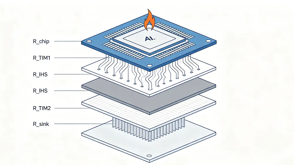
1. Understanding the Problem: Thermal Resistance Layers in AI Chips
Before evaluating specific materials, it helps to understand where heat actually gets trapped. The heat generated by an AI chip must pass through several layers before being removed by a liquid cold plate or heatsink.
From a thermal circuit perspective, the total thermal resistance can be expressed as:
R_total = R_chip + R_TIM1 + R_IHS + R_TIM2 + R_sink
- TIM1 sits between the bare chip die and the integrated heat spreader (IHS)
- TIM2 sits between the IHS and the cooling system (cold plate or heatsink)
At kilowatt power levels, even a microscopic 0.01 mm air gap on the chip surface creates localized overheating. Air has a thermal conductivity of only about 0.026 W/(m·K), which is essentially an insulator. These hot spots cause the chip to throttle its performance or fail entirely. That is why developing materials with high thermal conductivity and ultra-low interface resistance is critical for AI infrastructure.
Table 1: Thermal Interface Layers in AI Chip Packaging
| Layer | Location | Primary Requirement | Common Material Types |
|---|---|---|---|
| TIM1 | Between die and IHS | Ultra-low thermal resistance, good CTE match, good wetting | Liquid metal, CVD diamond, phase change materials |
| IHS (Heat Spreader) | Between TIM1 and TIM2 | Fast horizontal heat spreading, high conductivity | Pure copper, vapor chambers, CVD diamond films |
| TIM2 | Between IHS and cold plate/heatsink | Long-term reliability, pump-out resistance, easy assembly | Phase change materials, thermal pads, thermal grease |
2. Ranking and Analysis of AI Chip Thermal Materials
🥇 1st Place: CVD Diamond — The Ultimate Heat Spreader
Material Properties and Mechanism
Diamond has the highest room-temperature thermal conductivity of any known material. Its carbon atoms form a tight cubic lattice held together by strong covalent bonds. Lattice vibrations, called phonons, travel long distances through this structure with minimal scattering.
- Thermal conductivity: Natural diamond reaches about 2200 W/(m·K). Synthetic single-crystal diamond made by chemical vapor deposition (CVD) consistently achieves 1200 to 2000 W/(m·K) at room temperature. That is 3 to 5 times higher than pure copper.
- Coefficient of thermal expansion (CTE): Approximately 1.0 × 10⁻⁶/K, which matches well with silicon (about 2.6 × 10⁻⁶/K) and gallium arsenide. This close match prevents delamination and cracking during repeated heating and cooling cycles.

How It Is Used in AI Computing Centers
In AI data centers, diamond is used primarily as a heat spreader or directly as a chip substrate:
- Near-junction cooling: In 3D stacked packaging like CoWoS, a thin CVD diamond film (a few hundred micrometers thick) is bonded directly to the logic compute die. Its extremely high in-plane conductivity spreads hot spots instantly and lowers peak temperatures.
- High-frequency device substrates: For the RF communication and power supply systems around AI servers, diamond is used as a substrate for gallium nitride chips (GaN-on-diamond) to handle extreme heat generation.
Current Limitations and Future Path
The biggest barriers are cost and difficulty of machining. CVD diamond grows slowly and requires significant energy. Diamond is also extremely hard, so traditional mechanical polishing and dicing are very inefficient. The industry is now focused on high-efficiency laser cutting and ion-beam polishing. As manufacturing costs drop over the next several years, diamond is expected to become standard for high-power AI racks.
🥈 2nd Place: Graphene — The Ultra-Thin 2D Thermal Highway
Material Properties and Mechanism
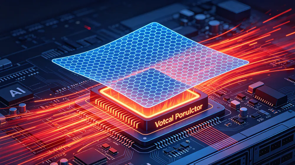
Graphene is a two-dimensional material made of carbon atoms arranged in a hexagonal honeycomb pattern. The carbon atoms are bonded through sp² hybridized orbitals, which gives the material its unique properties.
- Thermal conductivity: A suspended single layer of graphene has a theoretical conductivity of up to 5300 W/(m·K). In real engineering applications, multilayer graphene thermal films typically achieve in-plane conductivity between 1000 and 1500 W/(m·K).
- Anisotropy: This is the most important characteristic to understand. Phonons travel extremely fast along the plane of the graphene film, but conductivity perpendicular to the film is only about 5 to 20 W/(m·K).
How It Is Used in AI Computing Centers
Graphene acts mainly as a heat diverter in AI servers, using its excellent in-plane performance:
- Large-area heat spreading: AI server motherboards contain many high-power components beyond just the GPU or TPU, including voltage regulators, HBM memory stacks, and optical transceivers. Graphene films placed over these components spread localized heat horizontally to metal chassis or liquid cooling loop edges.
- Vertically aligned graphene (A-TIM): To overcome poor out-of-plane conductivity, advanced processes use magnetic or electric fields to align graphene flakes vertically. This creates an interface material with high through-thickness conductivity (up to 80 W/(m·K)) for use as TIM1.
Current Limitations and Future Path
Multilayer graphene films can delaminate or become brittle under long-term high-temperature and high-pressure conditions. Future research is focused on chemical doping to improve vertical conductivity and enhance wetting with chip metal surfaces.
🥉 3rd Place: Liquid Metal — Filling Microscopic Gaps Completely
Material Properties and Mechanism
Liquid metal refers to low-melting-point alloys that stay liquid at room temperature. The most common type is gallium-indium-tin alloy (GaInSn).
- Thermal conductivity: Pure metals and alloys have many free electrons, so they conduct heat primarily through electrons. Their thermal conductivity ranges from about 30 to 85 W/(m·K). While this is much lower than diamond, liquid metal has a completely different advantage.
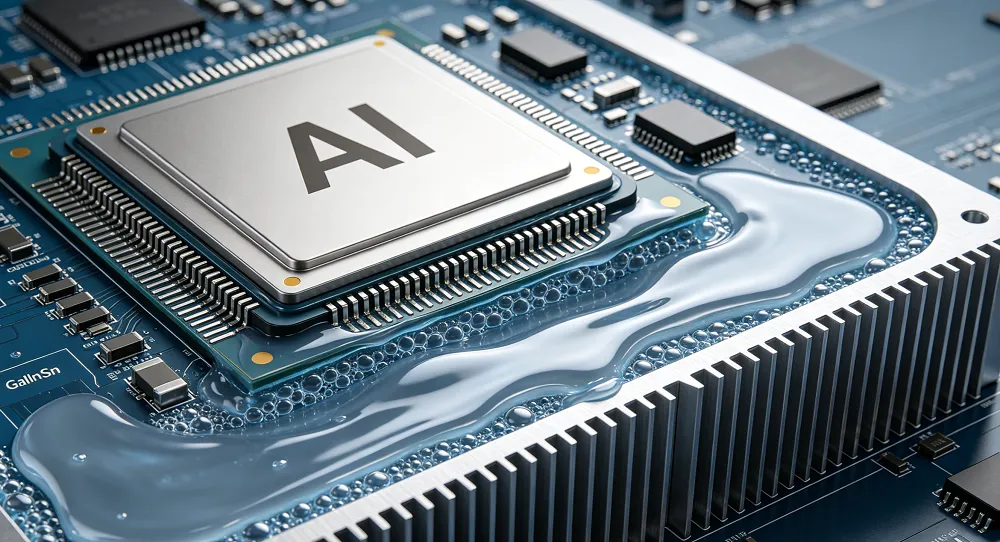
- Perfect microscopic contact: No matter how hard you press traditional thermal paste, microscopic air gaps always remain. Liquid metal, because it flows under pressure, wets the surface completely and fills every microscopic gap between the chip and the heatsink. This brings the contact thermal resistance very close to zero.
How It Is Used in AI Computing Centers
- Die-level (TIM1) applications: Some high-end custom AI accelerators and overclocked AI workstations use liquid metal directly on the die surface as TIM1.
- High-power cold plate interfaces: In direct-to-chip liquid cooling, using liquid metal between the GPU surface and the cold plate reduces the temperature difference dramatically. This allows the liquid coolant to exit at a higher temperature, which improves power usage effectiveness (PUE).
Current Limitations and Future Path
The main drawbacks of liquid metal are the risk of short circuits if it leaks and galvanic corrosion (specifically gallium embrittlement). Gallium reacts with aluminum and copper, causing the metal structure to become brittle and crack.
- Solutions: In the AI industry, copper heatsinks are typically plated with nickel as a barrier layer, and precision silicone gaskets are used to prevent leakage. Recently, “solidified liquid metal composite sheets”—where liquid metal is absorbed into a sponge-like polymer or a high-conductivity framework—have become a hot research area.
4️⃣ 4th Place: High-Conductivity Ceramics (AlN / BeO) — Electrically Insulating Workhorses
Material Properties and Mechanism
In the high-voltage power supply and high-speed signal areas of AI chips, materials must have both good heat dissipation and strong electrical insulation (low dielectric constant and low dielectric loss). Metals and graphene cannot be used here. Aluminum nitride (AlN) and beryllium oxide (BeO) are the leading options.
- Thermal conductivity: Industrial-grade AlN achieves 170 to 230 W/(m·K). BeO can reach 260 to 300 W/(m·K), though its production is heavily restricted because the powder is toxic.
- Insulation and matching: Both materials have high electrical resistivity, and their CTE (about 4.5 × 10⁻⁶/K) matches semiconductor chips well.
How It Is Used in AI Computing Centers
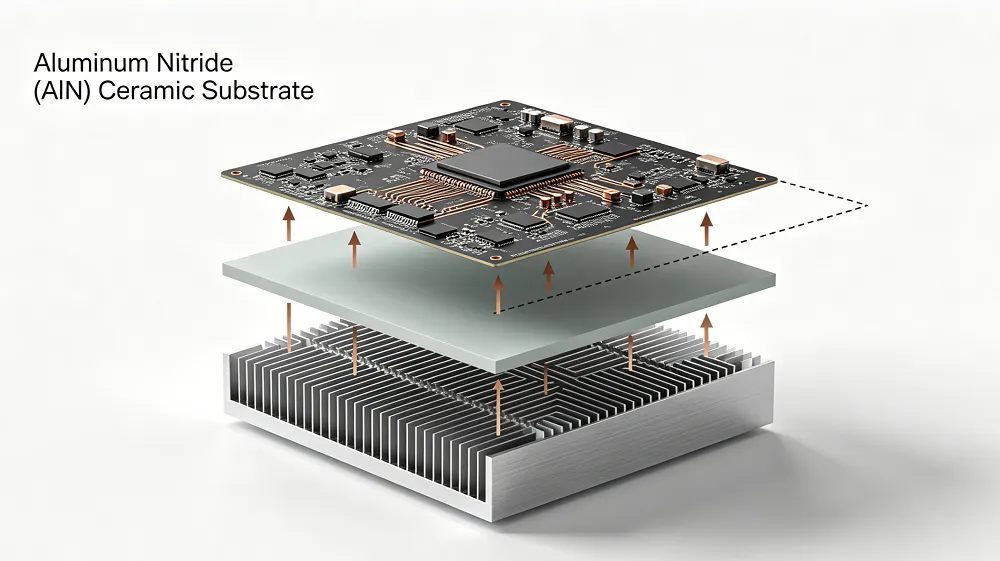
- AMB ceramic substrates: In AI server power delivery systems (such as MOSFETs and IGBT modules), ceramic sheets sit between the circuit board and the metal heatsink base. They isolate high currents while conducting heat downward.
- Advanced packaging substrates: Used as interconnect substrates for multi-chip modules (MCM), ensuring that multiple HBM stacks and compute cores do not crack due to uneven thermal expansion.
Current Limitations and Future Path
Ceramics are inherently brittle, require long processing times, and are costly to manufacture. The industry is currently exploring thinner silicon nitride (Si₃N₄) doping and modification technologies to achieve higher bending strength and a better balance between thermal conductivity and mechanical toughness.
5️⃣ 5th Place: Traditional Copper — The Solid 3D Thermal Backbone
Material Properties and Mechanism
Copper and silver have been workhorses of thermal management for decades. Their face-centered cubic lattices contain large numbers of free electrons that transport heat efficiently.
- Thermal conductivity: Pure silver is about 429 W/(m·K). Pure copper (such as C1020) is about 380 to 401 W/(m·K).
- Ductility and workability: Copper is very easy to machine, stamp, weld, and form into micro-channels. Its cost is also much lower than any of the advanced high-conductivity materials listed above.
How It Is Used in AI Computing Centers
Copper serves as the skeleton and circulatory system of AI server cooling:
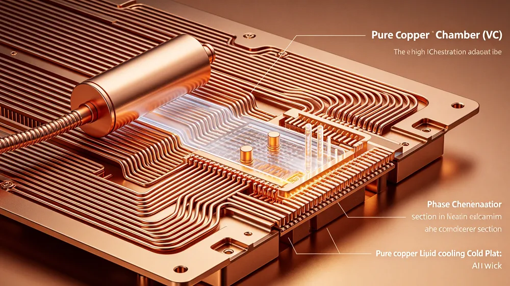
- Vapor chambers (VCs) and heat pipes: Sealed hollow copper chambers are filled with a working fluid (usually water). By using evaporation and condensation (phase change), they achieve an effective thermal conductivity several times higher than a solid copper block.
- Liquid cooling cold plates: The fluid control plates that sit directly on GPU surfaces, containing micro-channels at the millimeter or micrometer scale, are almost always made of pure copper.
Current Limitations and Future Path
Copper is dense and heavy. In massive data centers with tens of thousands of GPUs, all-copper cooling systems add significant weight, challenging the load capacity of server racks. The current trend is toward copper-carbon composite materials, which maintain high thermal conductivity while reducing weight by over 30 percent.
6️⃣ 6th Place: Phase Change Materials (PCM) — The Reliable Industry Standard for TIM2
Material Properties and Mechanism
Phase change materials (PCMs) are typically a polymer matrix (such as polysiloxane) densely filled with low-melting-point alloy powders, aluminum oxide, or boron nitride particles.
- Thermal conductivity: The bulk conductivity of the material itself is usually between 5 and 15 W/(m·K). That number seems low, but the real value of PCM lies in its dynamic thermal resistance.
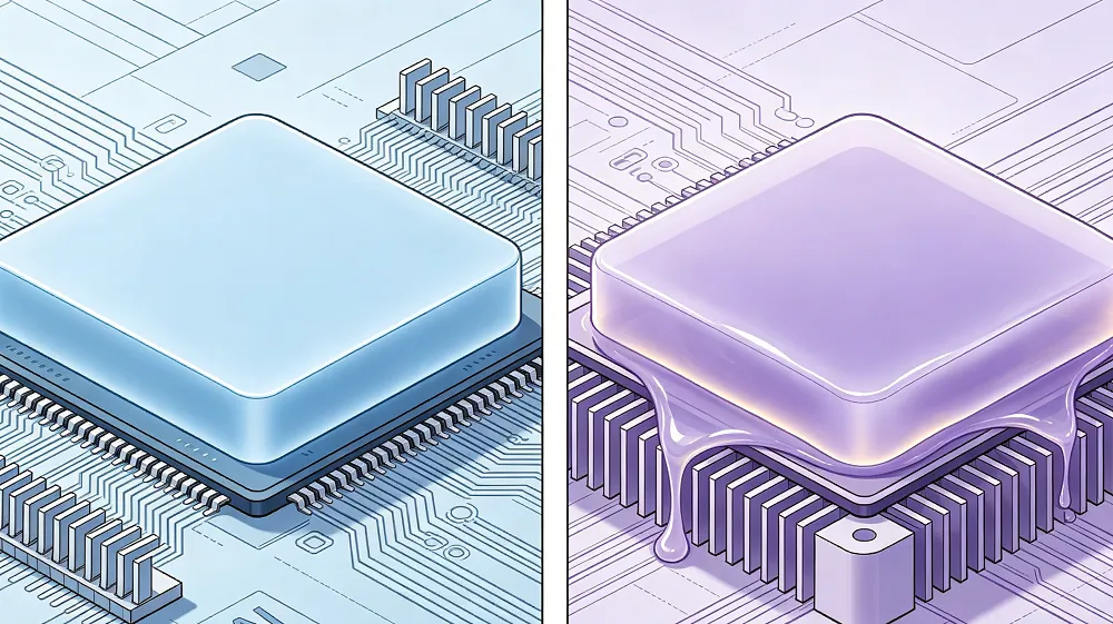
- Phase change behavior: At room temperature (below about 45°C), the material stays solid and acts like a pad. This makes it very easy for automated factory robots to pick and place during assembly. When the AI chip heats up and temperatures cross the phase change threshold, the material softens into a semi-fluid state. Under the clamping pressure of the heatsink, it pushes out trapped air and thermal resistance drops significantly.
How It Is Used in AI Computing Centers
PCM is currently the most widely used TIM2 material in AI data centers.
- Large-scale deployment: Products like Honeywell’s PTM series phase change pads are used across nearly all mainstream AI accelerator shipments. PCM elegantly solves two common problems with traditional thermal grease: the pump-out effect (grease expands when hot and contracts when cool, drawing in air and causing thermal failure) and drying out. Performance remains stable over tens of thousands of hours of server operation.
Current Limitations and Future Path
The main limitation is the low ceiling of bulk thermal conductivity. Next-generation PCM research focuses on blending trace amounts of graphene platelets or short metal fibers into the phase change matrix, aiming to push bulk conductivity past 20 W/(m·K) while keeping the material’s ability to soften and conform.
3. Comprehensive Comparison Table
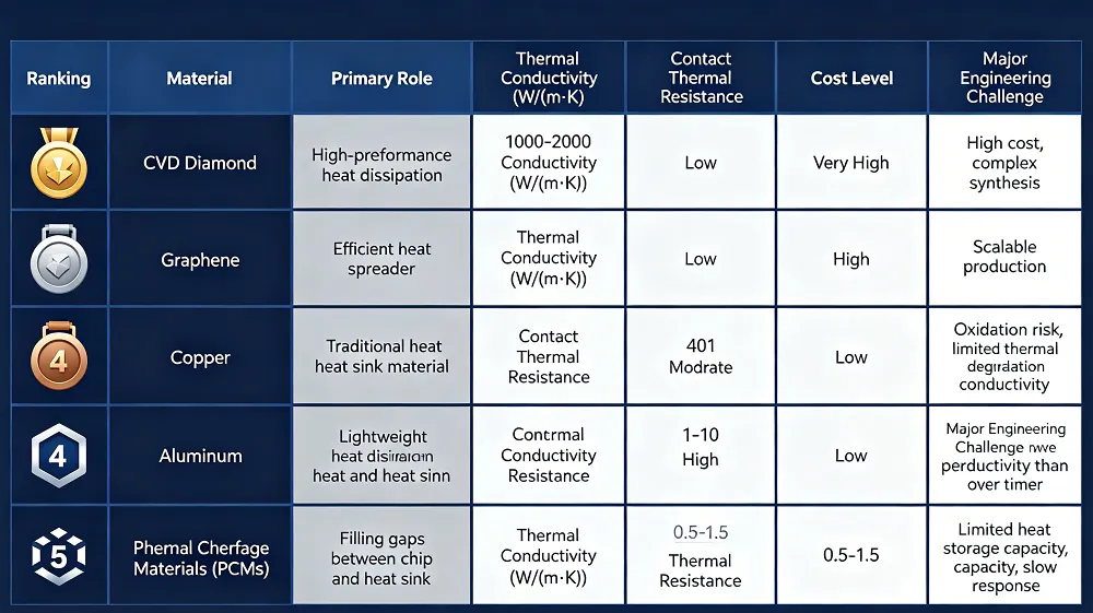
The table below summarizes the six materials, their roles, key properties, and major engineering challenges.
Table 2: Comparison of Six AI Chip Thermal Materials
| Ranking | Material | Primary Role | Thermal Conductivity (W/(m·K)) | Contact Thermal Resistance | Cost Level | Major Engineering Challenge |
|---|---|---|---|---|---|---|
| 🥇 1st | CVD Diamond | Heat spreader / TIM1 / Substrate | 1200 – 2000 | Very low | Very high | Laser cutting and polishing difficulties |
| 🥈 2nd | Graphene | Lateral heat spreader / A-TIM | 1000 – 1500 (in-plane) | Low (needs vertical alignment) | High | Extreme anisotropy; preventing delamination |
| 🥉 3rd | Liquid Metal | TIM1 / Cold plate interface | 30 – 85 | Near zero | Moderate | Electrical conductivity; severe corrosion |
| 4th | High-Conductivity Ceramics | Power module / packaging substrate | 170 – 230 (AlN) | Moderate | High | Brittleness; difficult to machine thin |
| 5th | Traditional Copper | Vapor chambers / cold plates | 380 – 401 | Low (depends on surface flatness) | Low | High density adds significant weight |
| 6th | Phase Change Materials (PCM) | Mainstream TIM2 | 5 – 15 | Low (after phase change) | Low | Low ceiling for bulk conductivity |
From Technical Selection to Stable Supply: Material Solutions from RBOSCHCO
The advanced materials mentioned above—CVD diamond, high-conductivity ceramics, and others—face two major challenges when moving from the lab to real engineering applications. First, there is a significant gap between excellent laboratory performance and reliable mass production. Second, supply chain stability and batch-to-batch consistency are difficult to guarantee. This is exactly the area where RBOSCHCO has focused its efforts for over twelve years.
As a manufacturer specializing in nanomaterials and high-end chemicals, RBOSCHCO has provided material support—from sample validation to large-scale delivery—to AI server manufacturers and packaging and testing companies across more than 30 countries and regions. Whether it is optimizing the low-melting-point alloy ratio of liquid metal or providing nano-scale filler particles for ceramic substrate modification, we offer customizable solutions.
Our technical team looks beyond just the thermal conductivity numbers. We also pay close attention to the practical challenges you may face on your production line—including material application processes, compatibility with existing cooling modules, and long-term reliability verification. If you are selecting materials for your next-generation AI chip cooling solution, or if you have specific engineering needs related to any of the technical approaches discussed in this article, please feel free to reach out.
RELATED POSTS
Advancing Materials Science: Comparative Study of Titanium Nitride, Chromium Nitride, and Tungsten Nitride
Development Status and Trends of Spherical Alumina
Microstructure and Electrical Conductivity of Titanium Carbide Aluminum Powder

Guide to Selecting the Right Metal Plates: Comparing Steel, Aluminum, Stainless Steel, Copper and Their Alloys
Silicon Nitride Bonded Silicon Carbide: High-Performance Ceramic Solutions for Advanced Industrial Applications
