Professional and high-quality metal alloys, ceramic products and concrete additives | RBOSCHCO
Silicon carbide (SiC), as the core material of third-generation wide bandgap semiconductors, has broken the performance bottleneck of traditional silicon-based materials with excellent characteristics such as high temperature resistance, high breakdown field strength, and high thermal conductivity, and has become a core supporting material in high-end fields such as new energy, 5G communication, and aerospace. Silicon carbide wafer, as the basic carrier for semiconductor device preparation, its quality directly determines device performance; Recrystallized Silicon Carbide, as a special derivative material, further expands the application boundaries of silicon carbide.
Core characteristics and classification of silicon carbide materials
1. Core Features: Performance advantages beyond silicon-based materials
Silicon carbide is a compound semiconductor formed by the covalent bonding of silicon and carbon. Firstly, the high bandgap width (3.26eV) is three times that of silicon materials, allowing it to maintain low leakage current in high temperature environments and operate stably above 600 ℃, while silicon materials can only withstand temperatures around 150 ℃; Secondly, the high breakdown field strength, reaching 2-4MV/cm, is 10 times that of silicon, which can significantly reduce the thickness of the device drift layer and improve power density; Thirdly, it has a high thermal conductivity of up to 120-270W/(m · K), which is three times that of silicon. It can quickly dissipate the heat generated during device operation and reduce the cost of the heat dissipation system. Fourthly, the high electron saturation drift speed is twice that of silicon, supporting the device to achieve high-frequency operation. In addition, silicon carbide also has the advantages of low conduction loss and high chemical stability, which are suitable for application requirements under extreme working conditions.
2. Main categories: Basic materials and derivative categories
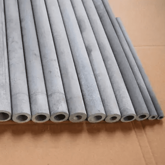
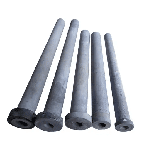
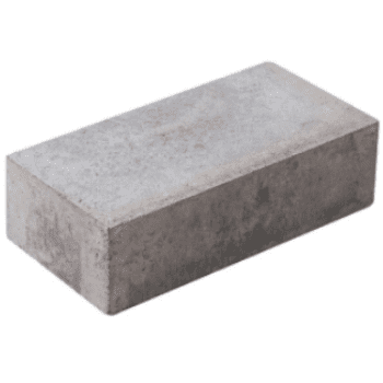
Silicon carbide materials are mainly divided into two categories: monocrystalline silicon carbide and recrystallized silicon carbide. In addition, there are also various types of materials, such as 3C SiC and 6H SiC, which are suitable for different scene requirements. Recrystallized silicon carbide (R-SiC) is a high-performance ceramic material made through a high-temperature solid-state sintering process, without the need for sintering additives. Its purity can reach over 99.5%, and it has high thermal conductivity, high hardness, corrosion resistance and other characteristics. It is mainly used in semiconductor equipment components, high-temperature kiln furniture and other fields.
Types and Preparation of Silicon Carbide Semiconductor Devices
1. Types and functions of core components
Silicon carbide semiconductor devices based on silicon carbide materials are mainly divided into two categories: power devices and RF devices, and are widely used in the fields of energy conversion and signal transmission. Power devices are currently the most mature category of applications, with core components including silicon carbide MOSFETs, Schottky diodes, IGBTs, etc. Among them, MOSFETs and Schottky diodes dominate the market. Silicon carbide MOSFET has low switching loss and high power density, which can greatly improve the efficiency of energy conversion and are widely used in new energy vehicle inverters and photovoltaic inverters; Schottky diodes have ultra-fast switching speed, no reverse recovery loss, and are suitable for high-frequency and high-voltage scenarios. RF devices are mainly composed of silicon carbide MESFET and HEMT, which rely on high-frequency characteristics and are used in fields such as 5G communication base stations and satellite communication to achieve efficient signal transmission.
2. Core Process of Device Preparation
The preparation of silicon carbide semiconductor devices is based on silicon carbide wafers, and the core process is divided into three steps: first, wafer pretreatment, cleaning and polishing of silicon carbide wafers to remove surface impurities and defects, ensuring that the surface reaches atomic level flatness; Next is epitaxial growth, which uses chemical vapor deposition (CVD) technology to grow a precise thickness of epitaxial layer on the wafer surface, regulate the doping type and concentration, and construct the core structure of the device; Finally, there is device manufacturing, where the source, drain, gate, and other structures of the device are formed on the wafer through processes such as photolithography, etching, ion implantation, and metallization. After packaging and testing, the finished device is obtained. The entire process requires extremely high precision, especially in epitaxial growth and defect control, which directly determines the reliability and yield of the device.
Key Technologies and Quality Control of Silicon Carbide Wafers
1. Core Technologies for Wafer Preparation
The current mainstream single crystal growth method is physical vapor transfer (PVT), which requires the sublimation of silicon carbide powder in a high temperature environment of 2200-2400 ℃ to grow a single crystal ingot on the surface of the seed crystal. The growth rate is extremely slow (0.1-0.5mm/hour) and is prone to defects such as microtubes and dislocations. After orientation, diamond wire saw cutting, grinding, chemical mechanical polishing (CMP) and other processes, single crystal ingots are made into wafers of different sizes. Currently, 6-inch wafers are the mainstream in the market, and 8-inch wafers are accelerating industrialization. In addition, epitaxial growth technology is also crucial for wafer preparation, requiring precise control of parameters such as temperature and gas flow rate to ensure uniform thickness and low defect rate of the epitaxial layer.
2. Key points of core quality control
The quality of silicon carbide wafers directly affects the performance of semiconductor devices, and the core control points include three aspects: first, crystal defect control, which requires controlling the micro tube density below 0.5cm ⁻ ² to reduce defects such as dislocations and layer faults, and avoid affecting the device’s conductivity; The second is dimensional accuracy control, ensuring that the wafer thickness is uniform, the surface flatness meets the standard, and the error is controlled at the micrometer level; The third is purity control, strictly controlling the impurity content in the wafer to avoid impurities affecting the carrier transport characteristics. At present, mainstream wafer manufacturers around the world are continuously improving wafer quality and reducing production costs by optimizing PVT growth processes and introducing new polishing technologies.
Full range applications of silicon carbide materials, devices, and wafers
1. New Energy Sector: Core Energy Conservation and Efficiency Enhancement Carrier
The field of new energy is the most widely used scenario for silicon carbide, covering two core areas: new energy vehicles and photovoltaic energy storage. In new energy vehicles, silicon carbide devices are used for main drive inverters and on-board chargers (OBCs), which can improve inverter efficiency to over 99%, reduce switch losses, and extend vehicle range by 10% -15%. Currently, Tesla, Xiaopeng and other car companies have installed them on a large scale; Silicon carbide wafers are the core carrier of automotive devices, supporting the popularization of 800V high-voltage platforms. In the field of photovoltaic energy storage, silicon carbide devices are used in photovoltaic inverters and energy storage converters to improve energy conversion efficiency and reduce equipment volume by more than 40%. Companies such as Huawei and Sunac have launched full silicon carbide solutions.
2. Electronics and Communication Field: Adaptation to High Frequency and High Voltage Scenarios
In the field of 5G communication, RF devices made of semi insulating silicon carbide wafers can work stably in high-frequency and high-temperature environments, supporting signal transmission for 5G base stations and improving communication distance and speed; In the field of industrial control, silicon carbide power devices are used in frequency converters and servo controllers, which can reduce energy consumption by more than 60% and improve equipment reliability. In addition, in the field of consumer electronics, silicon carbide devices are gradually being applied to fast charging devices to achieve miniaturization and efficient charging.
3. Special and high-end equipment field: extreme working condition support
Recrystallized silicon carbide, with its high purity, high temperature resistance, and corrosion resistance, is widely used in semiconductor equipment components such as crystal boats, spray heads, and electrostatic chuck bases, accounting for over 60% of the global market for high-purity silicon carbide components used in semiconductor equipment; In the aerospace field, silicon carbide devices are used in spacecraft power systems, radar equipment, and are suitable for extreme environments with high temperatures and radiation; In the field of rail transit, it is used for high-speed rail traction converter systems to improve energy conversion efficiency and reduce operating costs.
Development status of silicon carbide
At present, the silicon carbide industry is in a critical period of technological iteration and scale expansion. 6-inch wafers are achieving mass production, 8-inch wafers are gradually breaking through, device costs continue to decline, and application scenarios are constantly expanding. However, the industry still faces problems such as low single-crystal growth efficiency, difficulty in defect control, and dependence on imported core equipment. In the future, with the optimization of preparation processes and the promotion of domestic substitution, silicon carbide materials, semiconductor devices, and wafers will penetrate more high-end fields and become the core materials supporting the transformation of new energy and the development of the digital economy.
Supplier
RBOSCHCO is a trusted global Recrystallized Silicon Carbide supplier & manufacturer with over 12 years of experience in providing super high-quality chemicals and Nanomaterials. The company export to many countries, such as USA, Canada, Europe, UAE, South Africa, Tanzania, Kenya, Egypt, Nigeria, Cameroon, Ugand, Turkey, Mexico, Azerbaijan Be lgium, Cyprus, Czech Republic, Brazil, Chile, Argentina, Dubai, Japan, Korea, Vietnam, Thailand, Malaysia, Indonesia, Australia, Germany, France, Italy, Portugal etc. As a leading nanotechnology development manufacturer, RBOSCHCO dominates the market. Our professional work team provides perfect solutions to help improve the efficiency of various industries, create value, and easily cope with various challenges. If you are looking for Recrystallized Silicon Carbide, please feel free to contact us.
RELATED POSTS
Titanium Nitride Powder Shatters Boundaries: A Revolutionary Force in Global Industrial Supply Chains
Ceramic And Alumina Crucible Comparison: Which Should You Choose?

Revolutionizing High-Tech Applications: How Silicon Carbide and Tantalum Carbide Lead the Charge in Advanced Material Solutions

Unleash Unparalleled Potential: How Molybdenum Sulfide Solutions Are Sparking a Revolutionary Surge Across Global Industries

Why Is The Thermal Stability Of Ultrafine Zinc Stearate Emulsion Excellent When Used In PVC Products?
